
Taking Stock of SiC, Part 3: Breaking down the resistances of a SiC MOSFET
- Peter Gammon

- May 16, 2022
- 8 min read
Updated: Jul 18, 2022
In power device economics, a device’s resistance is a currency of choice. Scale down a MOSFET’s resistance and each die can be smaller, driving up device yields, and ultimately profits. Over 60+ years, every milliohm of a Si power MOSFET has been trimmed, achieving a fully optimised status quo. Meanwhile, just a decade on from the commercial release of SiC MOSFETs, there remains some big challenges yet to overcome before the same can be true of this technology, with manufacturers typically scaling down their specific on-resistance (Ω-cm2) by 30-40% with the release of each new generation of devices. Assuming the role of SiC-accountants, in this article we at PGC Consultancy run the numbers on today’s 650 and 1200V MOSFETs, arriving at a breakdown of the resistances that contribute to the total device resistance. This reveals the challenges, particularly in the optimisation of the gate oxide that are the key to its future optimisation.
This is the third post in which I am attempting to frame the present status of SiC MOSFET technology, both by comparing their competitiveness with Si, and also by exploring its own development. In Taking Stock of SiC, Part 1, I introduced the concept that reducing resistance in the design of a power MOSFET is key to reducing the size of a die. Die size reduction has the double benefit of increasing the number of devices produced per wafer, while the overall yield is also driven up, as defective areas of a substrate write off smaller die. In combination with innovation in the SiC substrate market – the move to larger substrates, and the potential to reuse substrates – continued reduction of specific on-resistance is one of the key methods available to drive down SiC costs.
Next, in Taking Stock of SiC, Part 2, I introduced the unipolar limit graph, reprinted below in figure 1, and populated it with the SiC MOSFETs, Si IGBTs and Si MOSFETs that PGC Consultancy have analysed for different customers over the last two years. In summary, after years of incremental improvement, the Si MOSFETs today are about as good as they are can feasibly get, their mapping on the graph demonstrating how close to the technology limit they reside, with virtually no excess resistance still to be shaved off. This means that for the chip manufacturer, they have maximised the number of devices they can possibly produce per wafer. This helps to explain the low cost of Si parts, given that multiple manufacturers have achieved this technology limit, notwithstanding the very low cost of Si substrates to begin with.
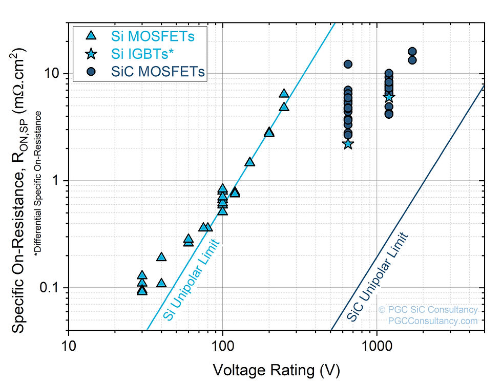
Today SiC MOSFETs provide great advantages over Si IGBTs, their low switching losses driving 650V MOSFET adoption for 400 V drivetrain inverters. However, as previously described, the benefits of using SiC only get better at 1200V. These devices reside closer to the unipolar limit, their resistance at 1200V being ≥14x greater than theoretically possible, compared to ≥33x at 650V, which translates to a SiC device with much lower switching losses lower conduction losses than the equivalent rated IGBT.
In this post, I will breakdown the resistances that contribute to a SiC MOSFET and explore the reasons why SiC devices are not yet close to their theoretical potential in the 650-1200V range, unlike mature Si devices.
SiC MOSFET Resistances: Naming the Culprits.
Figure 2 below illustrates all the major resistances that contribute to the total MOSFET resistance. Of these, the only resistance that scales with blocking voltage is the drift region resistance (RDr). Indeed it is in fact RDr that is plotted against a device’s blocking voltage to achieve the theoretical unipolar limit of a device. Hence, for a MOSFET to sit on the ideal technology curve, all the other fixed resistance components should be significantly smaller than RDr. This is the case with the Si MOSFETs above around 100 V, and hence these devices sit on the unipolar limit. However, should the drift region be thin enough, or if the other fixed resistances are large enough, then the device will not reside on the ideal technology curve, as per the Si devices below 100 V - and all the SiC devices plotted.

The largest fixed resistances, which are all independent of the rated voltage, include the highly doped substrate (RSubs), the channel resistance (RSubs) from where the current is forced against the oxide interface, and the resistance from the JFET region (RJFET) where the current is squeezed into a narrow channel between the device’s gate/body regions.
When laying out a die, ideally there would be minimal space that does not carry current. However, termination regions around the edge are required to maximise breakdown voltage, and gate pads needed to contact to the device. These add to a die’s footprint so skewing the specific on-resistance (resistance × area [ohms-cm2]) calculated. In accounting for the MOSFETs resistances, we discount this inactive area by reducing the total resistance by the % inactive area.
Finally, the package will add a small resistance to every device, as a few thin wire bonds are used to connect the semiconductor chip to the package. This affects most of the SiC devices analysed herein, but in fact, part of the reason that the Si devices are so incredibly good in Figure 1 is that this data comes from bare die, without resistances from packaging.
To understand the present state of SiC, one needs to consider each of these resistances. But first a question:
What voltage does a 650 V rated MOSFET breakdown at?

The answer to this is quite surprising. The best-in-class 650V MOSFET (as of late 2021), with the lowest specific on-resistance in Figure 1, actually breaks down at 1250V. The best-in-class 1200V MOSFET, which came from the same manufacturer, breaks down at 1550V. This can be seen in Figure 3.
While this might seem like a tangent from the theme of the article, of totting up device resistances, this overdesign, or derating, is critical. The trade-off between low on-resistance and high breakdown voltage, means that to achieve the optimal device, it should be designed to breakdown just fractionally higher that its rated voltage. Yet, as pointed out in a 2020 Wolfspeed article: “IGBTs are typically rated at 1.2 kV, with VDS breakdown voltage close to 1.25 kV. Wolfspeed’s SiC MOSFETs, while rated at 1.2 kV, typically have breakdown voltages several hundred volts higher.”
The best-in-class 650V MOSFET actually breaks down at 1250V.
At PGC Consultancy, we have independently tested the latest generations of SiC devices, from all the major manufacturers, and this drift region overdesign is universal, and these are not the largest breakdown voltages we have measured. The implication of this is that these devices will have a much higher drift region resistance than required (as RDr ∝ VBr^2.28), given that the most optimal resistance possible to achieve 1250V will be >4x greater than that for a 650V, the resistance at 1550V being at least 1.5x greater than at 1200V.
Why design for such a large voltage then? After all, Si devices aren’t derated to this degree, and with SiC real estate so expensive, there is much to gain by having the lowest possible resistance.
The primary reason for this appears to be gate oxide reliability. While SiC’s greatest strength is that it can withstand a high critical electric field, as this high field is supported at the semiconductor surface next to the gate oxide, it is problematic. Gate oxide leakage, and its reliability, is proportional to the electric field across it and Gauss’ Law dictates that the electric field in the oxide will be 2.6x greater than at the SiC surface. Therefore, were a 650V device really breaking down at 700V, then such a high electric field beneath the gate would cause yield issues, as a high percentage of devices would fail at during the gate stress burn-in qualification. By overdesigning the drift region to withstand a greater voltage, the result is a derating of the MOSFET. The 1250 V breakdown voltage of the 650V class MOSFET means that when the device is operated in a 400 V electric vehicle drivetrain, the peak field in the device will only reach one third of its highest possible value, ensuring long term gate reliability.
Analysing the resistances of SiC MOSFETs

Figure 4 shows PGC Consultancy’s model of the best-in-class devices shown in Figure 1. The clear difference between the two devices is the aforementioned drift region, so demonstrating the exponentially relationship between resistance and breakdown voltage. While the inactive area from the chip perimeter scales more weakly with voltage, all the other resistances are voltage independent.
The channel resistance is the largest fixed resistance. Both Si and SiC, when oxidised, produce silicon dioxide (SiO2), which is the insulator used in a MOS transistor. For Si, the process is nearly flawless, a near-perfect oxide results with a smooth interface between them. This means that electrons are barely impeded as they pass beneath this interface, and the resulting channel mobility (µCh; RCh∝ 1/µCh) of Si is 200 cm2/V.s. On the contrary, as SiC is oxidised, some of its carbon gets trapped at the SiO2/SiC interface, which bumps and scatters the electrons as they pass beneath. As a result, the channel mobility of SiC is around 20-30 cm2/V.s, and hence the channel resistance is 10x higher per unit length in SiC than it is in Si.
Substrate resistance comes from the N+ starting substrate of SiC, which has a relatively high resistivity. For example, Wolfspeed quote theirs as between 15-28 mΩ-cm. This is due to the ‘partial ionisation’ of the nitrogen dopant at room temperature, which means only a fraction of the nitrogen dopants in the substrate are electrically active. This is a difficult problem to tackle, so all chip manufacturers are exploring how far they can thin down SiC substrates post-fabrication from their original thickness of 350 µm. This varies between manufacturers from 100 to 180 µm right now. Note that again, the resistivity of Si substrates is around 1 mΩ-cm, at least 15x lower than SiCs.
A small JFET region resistance is also calculated, a value that can be minimised in planar designs by using a ‘charge storage layer’, a higher doped region beneath the gate. In trench designs, this is eliminated entirely (more in the next post).
Replotting SiC’s limits
Finally, we return to the unipolar limit graph of SiC, in order to visualise the current limits of SiC technology. Figure 5 contains the same theoretical SiC unipolar limit as Figure 1, and the same SiC MOSFET data. Added to this graph are the open circles, which are a recalculation of the best-in-class MOSFETs after the subtraction of an estimated packaging resistance, and using the area of only the active area of the die.

Also added to Figure 5 are PGC Consultancy’s estimates of the SiC channel and substrate resistances, represented as horizontal lines, as they are independent of voltage. A ‘Derated SiC Unipolar Limit’ represents the effect of having to derate a MOSFET to 50% of its potential the voltage rating to ensure gate oxide reliability.
Finally, the dash-dot line is the addition of the fixed resistances and the derated drift region, which results in a technology line that represents well 2021’s state-of-the-art SiC devices.
This shows very clearly the diminishing returns of scaling down SiC MOSFETs any further, how a 300V, or worse a 100V, SiC MOSFET would be little better than a Si device. This provides context for the 650V analysis provided in Taking Stock of SiC, Part 2. Conversely, it shows how SiC devices get closer to their optimal limits at higher voltage, at 3.3kV or above.
It also makes clear a roadmap for improvement, for lowering SiC device resistance further, and hence benefitting from the economics of a smaller die. Tackling the gate oxide is one of the key priorities for all SiC producers, a route to reducing channel resistance AND reducing derating. Meanwhile thinner substrates of lower resistance would help reduce losses further.
In summary, this analysis has revealed the reasons why SiC power devices, still in their very early, nascent years, are not yet as optimised as their Si counterparts. The problems highlighted in this article are ones that every chip manufacturer and research institute continues to work on and in the next post, we shall look ahead to some of the methods being used to further optimise the SiC MOSFET, including trench gates, innovations in the substrate including their reuse, and early work on alternative oxidation methods.


Comments